
Product Overview
The TC-Wafer wafer temperature measurement system adopts self-developed core technology, embedding high-temperature-resistant thermocouple sensors into the wafer surface to monitor and record temperature variation data during the wafer manufacturing process in real time, providing reliable data support for key process parameter detection, analysis and continuous optimization.
The system can withstand 1000°C high-temperature measurement, adapting to various extreme thermal process scenarios; relying on a multi-point layout scheme, it accurately collects temperature information at different positions on the wafer, outputs a complete wafer temperature distribution map, and quickly identifies process hazards such as uneven wafer heating and cooling. The equipment features excellent transient temperature tracking capability, capturing temperature dynamics and timing delays during heating, cooling and constant-temperature stages.
The product is compatible with 2-inch to 12-inch wafer specifications and is widely used in semiconductor process equipment such as PVD, ALD, CVD, annealing furnaces, ashing equipment, hot plates and heating dishes. It helps enterprises stabilize processes, improve production efficiency and chip yield, serving as a core testing tool for semiconductor thermal process calibration and process debugging.
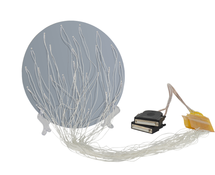
Product Specifications
Product Advantages
High Temperature
Thermocouple measurement range from room temperature to 1000°C, suitable for monitoring semiconductor manufacturing processes under extreme conditions.
Real-time
Provides accurate temperature data at specific positions on the wafer in real time.
Visualization
By placing multiple points on the wafer to collect temperature data, it provides the temperature distribution of the entire wafer, helping identify uneven heating or cooling issues.
Fast Response
Captures rapidly changing temperature dynamics, such as heating/cooling, constant-temperature processes, and delay times, as well as other key parameter variations.
Process Controllable
Continuous monitoring of wafer temperature changes during thermal processing helps adjust process parameters, improving production efficiency and ensuring product quality.
Applications
Thin Film Deposition Process Monitoring
Measures actual wafer surface temperature distribution, calibrates chamber temperature control, and stabilizes film thickness, stress and deposition uniformity.
Semiconductor Processing
Adapts to the full-range thermal processing steps of semiconductor manufacturing, follows the wafer into various process chambers, and obtains real wafer heating data. Supports equipment temperature control calibration, new process window development, mass-production process stability control and yield failure review, providing a reliable measurement basis for full-chain process parameter optimization in semiconductor manufacturing.
Thermal Process Optimization
Detects overall thermal uniformity of high-temperature processes, optimizes annealing and bonding temperature curves, and reduces warpage, bubbles and other process defects.
Lithography & Etching
Lithography: calibrates the true temperature of coating/developing equipment hot plates, controls photoresist volatilization rate, stabilizes CD line-width uniformity, and reduces pattern distortion and developing defects; Dry etching / plasma ashing: monitors dynamic wafer temperature rise in plasma environments, regulates etch rate, sidewall profile and selectivity, and avoids residue and uneven etching.